Migrating to Single-Chip Systems
by Kenneth H. Peters
System-on-a-chip designs are becoming increasingly popular in the embedded systems arena. What are they and how do the resulting system design changes affect traditional software development and debugging strategies?
Over the past decade, one of the more interesting advancements in embedded technology has been the move toward system-on-a-chip (SOC) implementations. The migration of discrete components into a single-chip footprint enables designers to take advantage of the cost, power, and speed that just arenˇŻt available in otherwise equivalent multi-chip systems.
Using a single-chip camera device as a case study, IˇŻll discuss the problems and pitfalls of writing and debugging software for this highly integrated device. IˇŻll also address the following questions:
- What issues remain after the SOC is produced?
- What concerns should you have as an early adopter?
- Are any software development issues unique to a single processor solution?
- What are the advantages and disadvantages to using SOC technology?
- What debug strategies are helpful?
Background
As market forces apply pressure on manufacturers to lower product costs, the technology available today and in the near future will continue to drive embedded solution providers to more highly integrated devices. Although cost and development time are higher for highly integrated devices, simply too many advantages exist for you not to pursue this technology. For the system integrator, the benefits of high integration include faster time to market, lower power consumption, higher reliability, and lower cost.Chip manufacturers are able to improve chip density in transistors and gates by decreasing the feature sizes on silicon. This improvement enables designers to place more functionality on a single die. Developers can integrate peripherals (such as USB or IEEE-1284), memory (DRAM, ROM, SRAM), DSP cores (ARM Piccolo), microprocessor cores (MIPS, ARM), and application-specific cores (MPEG, JPEG) into a single chip. Additionally, highly integrated devices such as these systems-on-a-chip sometimes involve the integration of proprietary third-party cores (intellectual property, or IP).
Although SOC manufacturers must overcome a variety of challenges to even begin to reap the benefits of integration, the software engineerˇŻs challenge starts when the completed silicon is available. Software development, integration, and debug present unique challenges as more functionality is packed into a single chip. One obvious challenge is visibility into the device. Many signals arenˇŻt connected to external pins, which limits the developerˇŻs ability to monitor interaction among the components of the chip. In some regards, to the software developer the chip is one very complicated black box.
Many phases of development use SOC technologies. Some companies are capable of producing highly integrated and application-specific ICs for their own applications. Although these companies are burdened with the cost of developing such devices, they have a competitive edge because they can directly influence development with regard to their own particular applications.
For most embedded designers, the ability to design and manufacture their own custom SOC is cost-prohibitive. These developers are left to choose from available silicon solutions one that best meet their needs.
What is system-on-a-chip?
Although the phrase ˇ°The System on a Chip Companyˇ± is a registered trademark, there are many companies offering application designers technology from specific SOC solutions to more generic integrated processor/ DSPs.The process of creating an SOC brings with it unique challenges. Some of the more notable among them involve integration of hard cores, whose layouts cannot be modified because they protect intellectual property or critical timing, and firm cores, which are modifiable but usually contain no intellectual property and can be difficult to support.
At the lower end of SOCs, hybrid solutions like the SH3-DSP and ARM/Piccolo processors are available as generic solutions that offer additional horsepower for those computational-intensive applications. Some examples are digital cameras, hand-held PCs, set-top decoders, and cell phones. Many of these processor/DSP solutions are integrated with little or no increase in cost to the end customer, as compared to their processor-only counterparts. These solutions are usually integrated with additional controllers and/or FPGAs for a particular application. These devices provide the system designer with additional flexibility, but may need to provide additional support through software or other ICs.
At the higher end of SOC offerings are the devices that contain the necessary functionality for specific applications. These devices are a fully integrated solution, in that very little additional chip support is required. There are two interesting SOC solutions targeted for the digital camera market. One is the COACH (camera on a chip) digital still camera processor from Zoran, and the other is DCAM-101 single chip for digital still cameras from LSI Logic. These single-chip solutions contain most of the necessary components to effectively implement a rich set of features for a digital still camera.
Generally speaking, you can loosely group SOCs into two categories: the generic hybrid solution and the integrated solution.
Generic hybrid solutions. HitachiˇŻs SH3-DSP solution, based on the SuperH microprocessor, is an integrated solution that provides an MMU and an on-chip memory controller. This chip is a hybrid and is best used for applications that require occasional support for either the SH3 or DSP. Although you have the ability to integrate DSP and SH3 instructions, the chip itself can only execute one or the other at any one time. The SH3 handles address generation and flow control, while the DSP performs instructions like multiply/accumulate. From a software development perspective, the SH3-DSP looks like a single processor.
A compiler is available that generates both SH and DSP instructions from C and remains software-compatible with other SuperH solutions. Hitachi and leading third-party suppliers offer complete hardware and software development and debug tools that are indispensable for system design. These integrated tool chains include simulators, assemblers, and GUI development and debug environments.
A digital cell phone is an ideal application for utilizing this hybrid solution. The function meld of MCU and DSP enable this application to be built with a single-chip solution. This chip provides both the micro-controller (SH3) capability for implementing user-friendly operating features and the DSP capability for efficient implementation of a speech codec, channel codec, equalizer, and communications protocol stack.
Integrated solutions. Highly integrated, application-specific solutions like ZoranˇŻs COACH represent a more complete SOC solution. This offering integrates all of the necessary functionality into a single chip and requires very little IC support. The COACH includes all the required hardware and micro-code to support: CCD/CMOS sensors, LCD controller, TV output, flash memory, USB interface, RS-232 interface, IrDA interface, and audio recording/playback.
Although this particular solution is highly integrated, a fair amount of software is required for its implementation. A core CPU isnˇŻt present (a digital signal processor is used instead), and the chip doesnˇŻt contain hard cores that implement image support functions needed for digital cameras. As with many SOC solutions, this particular offering comes complete with a ready-to-run software package to enable developers to quickly get digital camera functionality from their COACH solution.
True system-on-a-chip
LSI Logic is a supplier of custom high-performance semiconductors. The system-on-a-chip concept became reality several years ago with LSIˇŻs introduction of 0.38-micron 500K technology, which was later superceded by their 0.25-micron G10 and 0.18-micron G11 technology. The latest, G12, is the fourth generation technology to advance the system-on-a-chip approach. Using a feature size of 0.13 microns, G12 technology can provide 26 million logic gates (or 223 million transistors) on a 20mm x 20mm silicon chip. This enabling technology provides an extremely high level of integration for system designers.One particular market that has benefited from the advancement of integrated technology is the digital camera market. The development of digital still cameras requires advance technology and complex engineering. Among the more than 100 different digital camera models available today, many solutions exist. Some are based on proprietary chip sets, while others use commercially available solutions. Digital cameras bring the visible analog world into the digital world of microprocessors. Digitizing images from a CCD (charge coupled deviceˇŞa sensor used to capture light and turn it into readable data) through the system and ultimately storing the data as a compressed file requires a great deal of functionality.
LSI LogicˇŻs DCAM-101 single chip for digital still cameras is one of the most integrated SOC devices available, and contains all of the necessary functionality to control the functions of a digital camera. The core functions available in a typical digital camera include the following:
- CCD or CMOS sensor to capture image data
- LCD display of live and still images
- CompactFlash or SmartMedia storage device
- USB, IrDA, or serial communication channel for transfer of images
- Button support for operating the camera
The following is a list of features that might be required to operate the functions listed above:
- Image processing engine for image compression (such as JPEG) and image manipulation (such as color space conversion)
- Core processing unit (MIPS, PowerPC, ARM)
- Bus interfaces to support DRAM/ SRAM.
- DMA controller
- GPIO support for external input-like buttons
- CCD controller
- Display (LCD) controller
- ATA/SmartMedia support
- USB, IrDA, 1394 communication channels
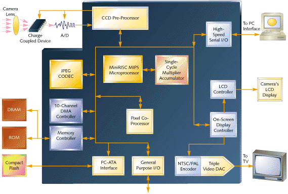
A block diagram of the DCAM-101 and the external devices required to engineer a digital camera is shown in Figure 1. The large shaded area in the figure contains devices within the DCAM-101. The only notable external devices required are DRAM, ROM, and CompactFlash. All of the necessary controller functionality is contained on-chip and hence it is a true system-on-a-chip design.
The MIPS CPU core and pixel accelerator coprocessor form the heart of the DCAM-101 device. In the following sections, IˇŻll describe how these components help facilitate SOC technology.
MIPS core
The MIPS core integrates an LSI Logic CW4003 processor core, which is a version of the MIPS R3000 RISC processor. The CW4003 implements a subset of the MIPS II instruction set. In an effort to make this SOC device more efficient, the DCAM-101 designers did some interesting things with this core.First, to reduce power consumption, a wait-for-interrupt (WAITI) instruction was added to the CW4003 architecture. Execution of this instruction causes the CW4003 to stop executing instructions and halts until the interrupt is observed.
Second is the utilization of a single unified cache. This cuts the processor I/O in half and reduces overhead outside of the CW4003 associated with address buses, data buses, and RAMs.
These types of modifications are common when integrating devices into a single chip. Notice that manufacturers have the ability to incorporate their own processor cores. This enables them to make specific design decisions for key components because they own the IP.
When using system-on-a-chip technology, you must pay specific attention to the core processor. This part of the device drives many of the other design decisions. Depending on the processor core architecture, you will have different development strategies. This core utilizes one of the more pervasive RISC coresˇŞMIPS. This architecture has some interesting characteristics that lends itself to SOC designs.
The MIPS architecture is backward-compatible, for the most part. That is to say that MIPS I instructions are supported on a processor that supports MIPS II, and MIPS III supports instructions that are supported for MIPS II, and so on. One of the nicer features about the MIPS architecture is that all MIPS I processor architectures utilize the same memory map.
The MIPS I architecture has two address spaces: virtual and physical. The virtual address space is partitioned into four fixed-size segments: kuseg, kseg0, kseg1, and kseg2. Segments kuseg and kseg0 are uncached and kseg1 and kseg2 are cached. A virtual address consists of both a segment identifier and an offset. The three most significant bits of the address specify the segment and the least significant bits specify the offset. For example, the address 0xA000FF00 specifies an address in segment kseg1 with an offset of 0xFF00.
The DCAM architecture doesnˇŻt employ a memory management unit (MMU) or translation look aside buffer (TLB). When no TLB is present, the mapping for segments kuseg and kseg2 is vendor-specific. The DCAM-101 maps all segments into the same physical address (0x00000000 to 0x20000000). Figure 2 shows the memory map specific to the DCAM-101.
All of the devices for the DCAM-101 are memory mapped. That is to say that all registers can be accessed through an associated address. No complicated command/data registers are involved. No advance setup is required. Access to a given register is performed in its associated memory address. Most of the work involved in programming the DCAM-101 requires the manipulation of registers.
Coprocessor support
When utilizing SOC designs, understanding how you might interface to additional processors outside of the core CPU is important. The specification for the MIPS architecture is interesting in that it defines four coprocessor units (CP0, CP1, CP2, and CP3.) A coprocessor is an auxiliary processing unit that operates in coordination with the MIPS CPU. Furthermore, each coprocessor may have an instruction set, 23 general-purpose registers, and 32 control registers. Each coprocessor is described below:
- CP0ˇŞis known as the system control processor and provides support for memory mapping and exception handling
- CP1ˇŞsupports floating-point operations
- CP2/CP3ˇŞare undefined and are intended to permit special-purpose engines
Software interacts with each co-processor using the MIPS instructions: swcn, lwcn, mtcn, mfcn, ctfn, cftn, bcnt, bcnf, and copn, where ˇ°nˇ± is either 0, 1, 2, or 3, to specify a coprocessor. For example, the instruction swc2 is ˇ°Store word to coprocessor 2,ˇ± and lwc2 is ˇ°Load word to coprocessor 2.ˇ±
The DCAM-101 uses the user-defineable coprocessor 2 (CP2) interface to access a hardwired, pixel-processing accelerator. This coprocessor converts CCD pixel image data into a format appropriate to JPEG compression or for an LCD display. The interesting aspect of this coprocessor is the powerful hardware support available to perform color-space conversion (such as RGB to YCrCb), pixel interpolation (SIM14, SIM20), up/down sampling of pixel data, and a variety of merging/rearranging register data functions used to set up data for JPEG or LCD display.
When the pixel coprocessor is coupled with the JPEG engine, the power of SOC designs becomes apparent. For example, a complete software-only solution for JPEG compression on the DCAM-101 (including both color space conversion and JPEG processing) can process a 640 x 480 CCD image in about four seconds. The DCAM application-specific hardware accelerators process the same image in fewer than 200ms.
Early access SOC development
Time-to-market considerations may make it necessary to exploit early-access silicon. The software developer must recognize that the benefits of using early access SOC technology does not come without a price. Developers may have to contend with multiple revisions of the SOC as integration issues are being resolved. Although many early versions are fully functional, some may experience revisions where whole subsystems may not be available and may require some clever software solutions until the problems are resolved. Typically, final resolution may not occur until the next revision, which could be three to six months away.Although early access provides developers with an inside look into a particular technology, software developers risk contending with a potentially unstable environment. One classic problem in early SOC development is the risk encountered during testing. For example, test vectors that designers provide to the silicon foundry may all pass, but the chip may not function properly in the application.
Test vectors are a defined set of logic states for all input pins of the device for every clock-cycle. A set of corresponding output vectors verifies that the correct responses are generated for a given set of inputs. These test vectors are then run against a simulation of the design database and the output is compared with the expected results. As you can imagine, manually generating these test vectors can be a daunting task. In fact, generating test vectors for some projects requires just as much time as was required for the design itselfˇŞwhich, in turn, doesnˇŻt leave a lot of time for debugging.
Fortunately, some of the co-verification tools available today provide simulation that enables the actual driver software to exercise the SOC design itself. This helps to facilitate more test coverage, as the simulation is used to reflect real-world environments.
An additional approach to verify SOC designs is to use logic emulators. The cost associated with such an emulator can be prohibitively expensive. While microprocessor emulators range from $4,000 to $30,000, a logic emulator may run to hundreds of thousands of dollars. Some estimates are that it costs about $.50 per gate to emulate a complete SOC solution. Although this solution does provide additional insight into the SOC design, critical timing issues and signaling delays make it difficult to fully emulate a particular solution. Furthermore, the amount of time to complete an effective simulation can be measured in hours, days, and sometime even weeks.
The average embedded developer doesnˇŻt have the resources required to purchase simulation tools in excess of $100,000. In the following sections, we will examine the resources and address the issues for developers that are integrating an off-the-shelf SOC device. Using the DCAM-101 as a reference, we will explore the software development and debug for an SOC.
Software development and debug for SOC
An SOC attempts to integrate different design technologies into a single chip. The development methodologies familiar to board-level design engineers may not be applicable for these designs.Before an SOC can be integrated into your application, you must conduct a careful evaluation of the design and development strategy. Software and hardware development around SOCs bring many challenges, along with the selection of tools, training, and methodologies. Some development tools aim at creating an algorithmic abstraction of the embedded system itself. Tool developers such as Synopsys, i-Logix, ObjecTime, and Cadence are creating front-end partitioning tools to help system architects and designers decide how to partition these algorithms into hardware and software.
The development of highly integrated systems has put more of an emphasis on hardware/software co-design. System integrators are beginning to see the benefits of merging hardware and software disciplines. There is enough evidence to suggest that the old way of debugging (ˇ°de-buggingˇ± defects out of the design) may not be as cost effective as hardware/software co-verification. Co-verification enables the hardware and software design teams to detect and correct design flaws before the commitment to silicon is made.
The hardware within an SOC is expensive to produce (it is a labor- and capital-intensive process that takes many months or years). Because of the tremendous cost, a large amount of simulation is performed during the chipˇŻs design phase. As a result, the actual silicon is nicer to work with than a more traditional hardware design. The components within the SOC are known (or strongly believed) to work together as they should long before a software engineer gets his or her hands on the chip. Writing low-level software is more of a task of deciphering the manual than worrying about whether a particular device is working and properly interfaced to the CPU.
Of course, software development for SOC-based designs does bring with it its own set of unique problems. But itˇŻs possible to plan for these problems by taking the following steps:
Choose software developers with a multi-disciplinary knowledge. SOCs are highly integrated and often have a tightly coupled interface from device to device. Simply reading and writing registers isnˇŻt enough; understanding the technology the device is trying to implement is often more important. For example, programming a JPEG engine might be a simple matter of loading up the engine with a variety of tables (Quantization, Huffman, and so forth), setting up a couple of DMA transfers, configuration, and feeding it some data. The real issue for the software developer is understanding the JPEG engine itself.
Develop a rich set of test and diagnostics. As with most designs, a rich set of diagnostic tests helps to verify the fundamental design. Remember that with SOC designs, you have very little or no visibility into the device. Most of the tests and diagnostics for these designs are geared for data verification that can read and write registers. Develop tests that drive known data into the chip with known results to verify proper operation. When you feed these devices real-world data, youˇŻll have the confidence that the device properly handles the data flow. These tests also help in regression tests, in the event that you require a new revision of the SOC.
Expect problems and plan on them. This point is most appropriate for early adopters. Systems-on-a-chip are complex and may require several revisions to get all the kinks worked out. Becoming an early adopter is a great way to gain in-depth knowledge of a design, but this should be met with patience and understanding.
Take advantage of the chip features from the very start. Design software that exploits the special features of the design. One of the bigger advantages is speed. Many devices support direct DMA from device to device or support multiple data and address buses. If the architecture is designed for pipelining, then design for pipelining up front. If you decide to take a crawl-walk-run approach and design in SOC features over time, you may never be able to take full advantage of the SOC design.
Employ CPU/DSP solutions that are highly integrated. If you have little or no experience working with a DSP but want to take advantage of these types of devices, consider solutions that provide a seamless software solution. For example, the SH3-DSP utilizes a single instruction stream and can generate DSP instructions directly from C. No complicated setup or navigation is required to employ the DSP.
Develop support tools. Because SOC devices tend to be fairly bug-free, you will spend more time working to manipulate register configurations. Systems-on-a-chip are mostly controlled through memory-mapped devices and provide an abundance of configuration options. For example, clock selection and timing parameters can be changed with a new value in a register and selected features can be enabled or disabled with the flip of a bit. Design software that enables you to change register configurations at run time. Changing register configuration and observing the behavior is sometimes the only way to gain understanding of a particular section of an SOC.
Understand data flow. Because SOCs tend to exploit the close proximity of internal devices, they tend to shuffle data from one device to the next. Understanding the data at each stage of processing is crucial to understanding the interaction inside the SOC. Develop tools that enable you to save data for each stage along the way. For example, in a digital camera, it is helpful to see the data directly from the CCD, and before it is sent to the JPEG engine for compression, or to see data directly after compression.
Use I/O features for debugging. Most system-on-a-chip designs provide general-purpose I/O (GPIO) for interacting with the outside world. These GPIO lines can provide critical timing information through toggling a line and monitoring it with an oscilloscope or logic analyzer.
Use background debug tools. Many system-on-a-chip designs incorporate a background debug port. Perhaps the most useful tool is a JTAG-based device for controlling the functionality of an embedded core. For example, ARM provides an Embedded ICE for this purpose. This feature lets the developer see activity inside the SOCs.
By way of comparison
Most embedded developers are familiar with applications that use board-level solutions (as opposed to SOC). Developing software for embedded systems that utilize discrete components gives access to most of the signals between these various devices.The following lists outline some advantages and disadvantages of a typical board-level system compared to an equivalent SOC system. The advantages of board-level development are:
- Board-level debugging has the distinct advantage of visibility. When a particular board-level anomaly arises, many possible workarounds present themselves. The developer can physically modify the board by cutting traces, lifting pins, and adding wires
- Board-level development enables individual devices to be replaced or upgraded. If a particular device goes bad, itˇŻs fairly easy to replace
- Board-level debugging presents visibility to signals from the various components. The signals that travel from device to device are visible to analysis tools such as oscilloscopes, logic analyzers, and the like
Disadvantages of board-level development include:
- Board-level systems with separate DSP and CPU often require different tool chains to support each device. Furthermore, the delineation of these devices makes CPU-DSP interaction problems difficult to resolve
- Having a board with several discrete components can cause problems during the latter part of the support stage. As individual components become scarce or unavailable, finding replacement parts can be difficult. This may also result in software modifications to support the new ˇ°replacementˇ± part
Advantages of SOC:
- Hybrid CPU/DSP integrated devices are supported by the same tool chain. In some cases, as with the SH-DSP, the complier seamlessly weaves together code instructions for the CPU and DSP
- Once a particular SOC is fully debugged and functional, the developer can be assured that all devices in the SOC work as documented. Furthermore, all of the signals have been pre-qualified, so we know that the device is operating properly. This in turn means that most of the problems encountered will be related to software
- With highly integrated SOCs, hard cores can be used to implement highly computational functions in hardware. For example, the DCAM-101 provides a JPEG engine, which dramatically outperforms an equivalent software solution
Disadvantages of SOC:
- Obviously, with this highly integrated device, you canˇŻt simply replace a particular deviceˇŞyou must replace the entire SOC. For example, if the CCD controller isnˇŻt working properly, you can continue to develop without CCD functionality. Otherwise you must replace the SOC itself
- Depending on the integrated device, you must be satisfied with how it was designed and integrated. For example, the JPEG engine of the DCAM-101 supports baseline-DCT only. If a more progressive JPEG solution is required, you must either select an alternate SOC or augment the device with software
- Visibility into the SOC is limited. If it doesnˇŻt support some kind of JTAG or BDM, visibility is limited to external pins. If an RTOS with a software-based debug agent is enabled, then reading of internal devices can be done through the source-level debugger
Software development
The software development process for SOC is similar to the one used to develop single-board computers. Software development starts with the processor and works outward. Most SOC designs contain a CPU core that is surrounded by a variety of devices. If we look at the typical software development process and apply it to SOC designs, you can see many similarities. The following list represents the typical high-level software development process for SOC designs:Selection of SOC for given design. Commitment to a particular SOC has a very large impact on your design. You cannot replace a given component within an SOC. A detailed analysis of your application and proposed SOC designs should provide the best match. If the application can survive without the need for an SOC, you might consider this option.
Identify core processor. Most single-chip designs incorporate a processor core such as MIPS, PowerPC, SH, or ARM. Each processor architecture has some distinct advantages and disadvantages. Some cores may not be appropriate for given applications. For example, the DCAM-101 doesnˇŻt contain an MMU, and therefore will not support Windows CE. Memory interfaces and DSP utilization may be a factor. If you need specific DSP control, you might select an ARM/Piccolo that enables each device to run simultaneously.
Selection of tools. Select tools that provide the highest level of integration. Tools that are generated by the manufacturer of an SOC tend to provide more insight into the SOC device. Generic tools can work with a variety of devices, from SOCs to processor chips. With the DCAM-101, you can use the same development tools used for any MIPS processor.
Selection of RTOS. The highly integrated SOC designs require no small amount of coordination. Many of these devices have multiple DMA channels and interrupt sources. Using an RTOS enables the developer to provide the proper amount of control over the system.
Port RTOS. Getting an RTOS up and running for your SOC design enables a firm foundation for the rest of the development. It may also be helpful to incorporate a debug engine so that source-level debugging will be possible. A source-level debugger gives you visibility into the device. Internal memory and register settings can be inspected and modified using the debugger. Porting an RTOS often begins by selecting one with a core similar to the one used in the SOC. Developers may select an RTOS that has already been ported to a generic processor (like MIPS).
Develop application code. Development of the application is similar to traditional development, with the advantage of knowing that all of the features of the SOC hardware are operational.
Test and debug. Again, this is the beloved edit-compile-debug approach. Keep in mind that many SOC solutions do not provide an emulator, and software simulation of your design can be time consuming and expensive.
A key role
System-on-a-chip designs will play a key role in the future advancement of embedded systems. As the development of these complex systems becomes mainstream, tool support and robustness will become commonplace. Systems that are designed to maximize the features of an SOC will reap the biggest benefits. Whether your design incorporates a hybrid processor/DSP or a full-blown SOC, you can realize many advantages over traditional board-level designs. espKenneth H. Peters is a principal member of technical staff and works in the Embedded Systems Technical Competency Center for Questra Consulting. He has math and computer science degrees from State University of New York at Geneseo. Ken has almost 15 years of experience in embedded system development, from motion control to digital camera design. Prior to joining Questra, Ken spent time developing video measure machines at Optical Gaging Products in Rochester, NY.
Illustrations Figure 1
Figure 2
References and Useful Sites
www.zoran.com
www.lsilogic.com
www.hitachi.com
www.microsoft.com
Return to Embedded.com
Send comments to: Webmaster
Copyright © 1998 Miller Freeman, Inc.,
a United News & Media company.