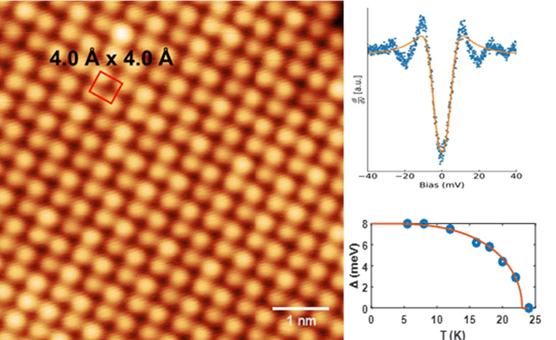
The low temperature scanning tunneling microscope (STM) with electronic transport measurement is employed to explore novel characteristics of electronic state and physical properties in superconducting film and nanomaterials, including the high-Tc superconductor from the latest theory and calculation, topological superconductor, transition metal dichalcogenides (TMD) and oxides, functional materials made up of simple materials with artificial modification. Combining the basis of theoretical calculations with the integrated UHV-cluster platform, deep insights of the phenomena (superconductivity, topological properties and quantum state, etc.) would be revealed from experimental results of STM, Angle-resolved Photoemission Spectroscopy and transport measurement, which is characteristic idea of our study. For one thing, theoretical calculation predicts the existence of novel materials, and implies the possible experimental conditions. For another, with the advance of integrated UHV cluster system, different kinds of equipment (STM, Angle resolved photoemission spectroscopy and transport measurement) are used easily and comprehensively without the risk of contaminating the sample; Hence, deep insights would be purely extracted from complicated phenomena like superconductivity, topological transport and quantum state and so on.n addition, we will focus on the manipulation of the superconducting physical proprieties and quantum state in order to improve the performance of solid-state quantum computation devices based on these novel materials.

We will manipulate electronic states and quantum properties in low-dimensional materials, for instance, the reconstruction on semiconductor, molecular chains and TMD nanoribbon, etc.. The electronic ground state and phase transition are manipulated by defects, strains, doping and Moiré potential in the material, or the artificial way of electric field from STM tip and bending in materials. After that, we would like to realize the electronic state manipulation in simple electronic system, which is similar to the traditional strongly correlated electronic system where different order parameters co-exist and compete. These researches can provide a new way for the future design of quantum devices based on the simple electronic system, such as silicon-based materials.
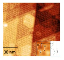
The ultra-high vacuum (UHV) cluster system is widely employed to fabricate novel low-dimensional materials and superlattices. Two smart objects are proposed:1. Novel two-dimensional honeycomb monolayers produced by the technology of breaking through the thermodynamic limitation and fine tuning of liquid-solid source;2. Novel low-dimensional materials and superlattices fabricated by the combined technologies of molecular beam epitaxy, chemical vapor deposition and mechanical exfoliation. It will broaden the classification of the high-performance materials for future nanoscale optical devices and quantum devices.
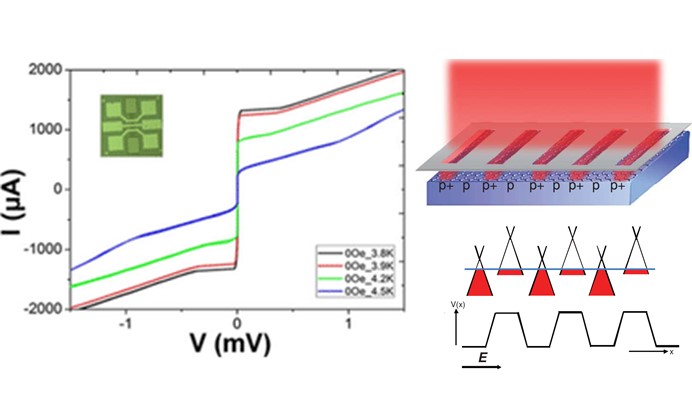
Development of in situ fabrication techniques for preparing micro-nano vertical heterojunctions in vacuum instead of traditional process of nanodevice production, We would like to develop two objects with our own characteristic: 1. Developing the functional photoelectric heterojunction and functional device by local ferroelectronic field; 2. Josephson vertical junction devices for manipulation of the Majorana fermion. The research will expand the area of device development and application of various low dimensional materials.

Because of the quantum and energy fluctuation in vacuum, the Casimir force emerge between two pieces of neutral metal pieces. A new type of scanning Casimir force detector will be developed to measure interaction between different low-dimensional material surfaces based on atomic force microscopy, which could be a practical approach to detect different dielectric functional excitation and quantum effect by external electromagnetic waves and plasmonics.

The industrial preparation of low-dimensional materials and design of devices are hot topics in recent years. We cooperate with Anhui coal research institute to explore new energy utilization of coal, such as preparing high-quality graphene, carbon nanotubes. Cheap ingredients are processed into high-technology materials, which provides promising future of industrial application of low dimensional materials.